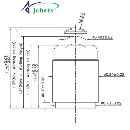


Specifications of High Speed Pogo Pin
| Parameters | Values |
|---|---|
| Characteristic impedance | 50Ω ± 5%, |
| Bandwidth/frequency range | DC – up to 10GHz, custom, |
| Insertion loss | ≤ 1.2dB @ 10GHz, |
| Return loss/VSWR | Return loss >15dB @ DC-10GHz, VSWR ≤1.5:1, |
| Crosstalk | Adjacent channel suppression ≥ 40dB @ 10GHz, |
| Differential impedance | 100Ω ± 5% for USB/PCIe, 90Ω ± 5% for memory, |
| Bit error rate | ≤ 1e-12 (only 1 bit error allowed per terabyte transmission), eye diagram template pass rate ≥ 99.9% |
| Contact resistance | Initial value ≤ 20mΩ (high-performance customization can reach <5mΩ); Within the lifespan, ≤50mΩ |
| Insulation resistance | ≥ 1,000MΩ @ 500V DC, |
| Withstand Voltage | 500V AC/1 minute without breakdown or flashover, |
| Rated current | 1A -2A (standard), Partial design can reach 5A-11A (balancing high speed and power supply) |
| Contact capacitance | ≤ 0.1pF, |
| Thickness of gold plating layer | ≥ 3μm, Extreme reliability requirement ≥5μ m to 10μm |
| Bottom layer of coating | Nickel bottom layer ≥ 5 μ m, blocking copper diffusion and enhancing wear resistance |
| Dielectric constant of Insulating materials | Housing material Dk≤3.2 @10GHz, Df ≤ 0.002 (low loss, LCP) |
| Mechanical life | 500,000 to 1M insertions |
| Spring force | 20gf – 60gf per high speed pogo pin |
Catalogs of High Speed Pogo Pin
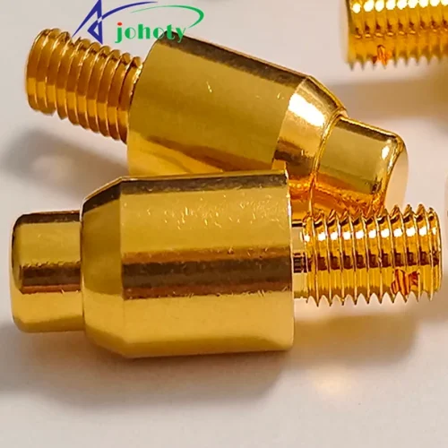
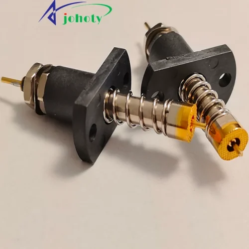
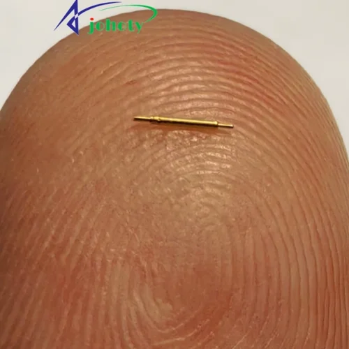
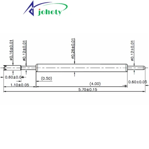
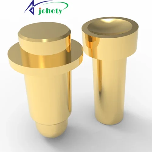
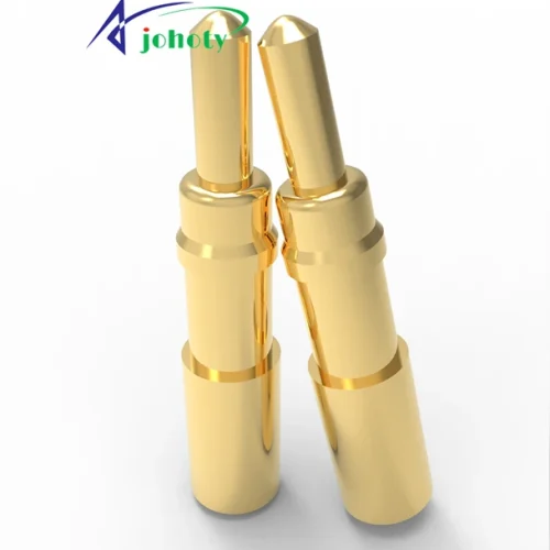
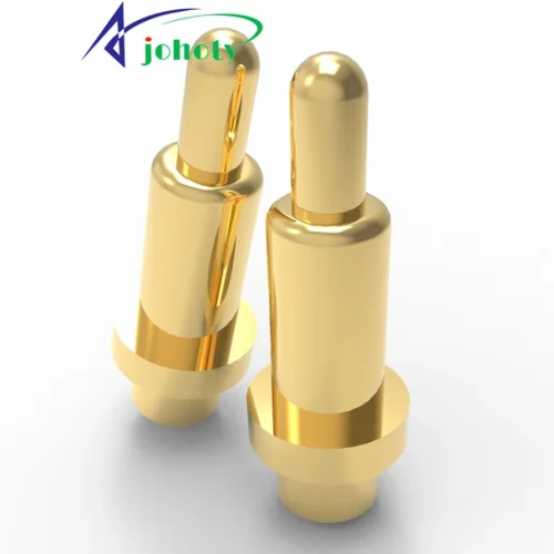
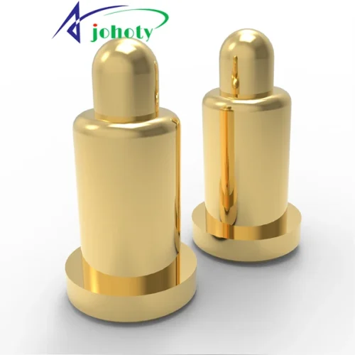
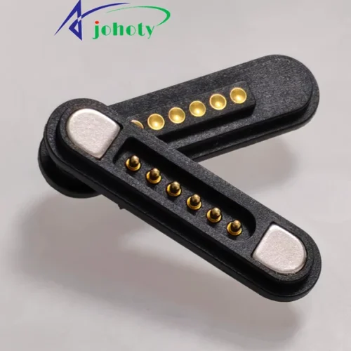
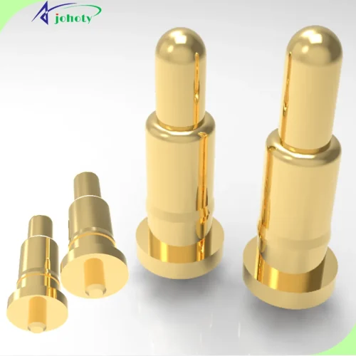
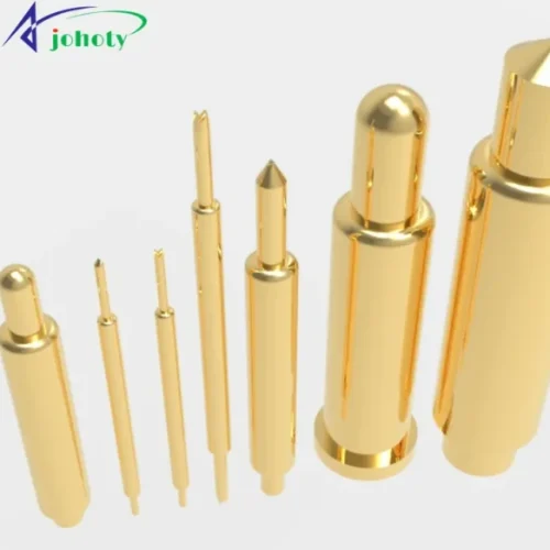
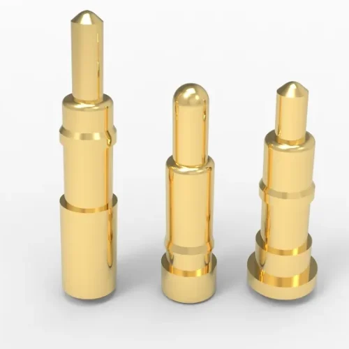
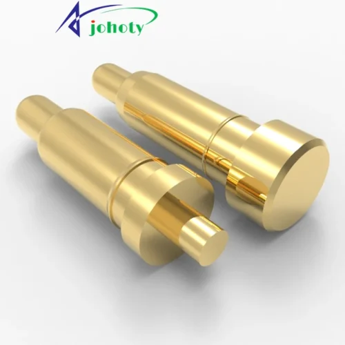
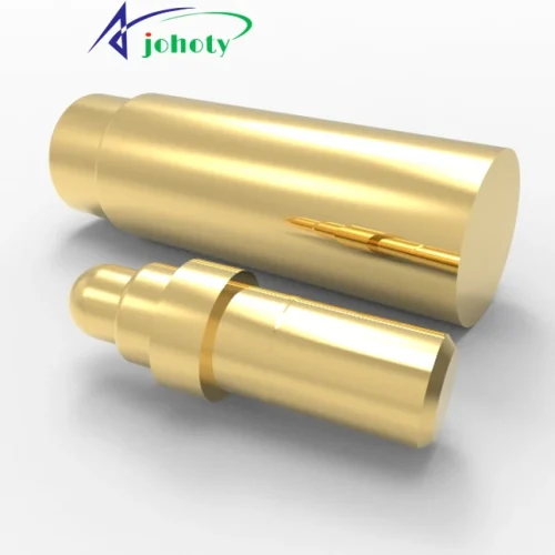
High speed pogo pin, the most crucial factor is the electrical parameters, such as extremely low contact resistance, etc. Mechanical consistencies and precision are to determine the stability and phase. Johoty can customize high speed pogo pins for you based on the following 5 types of shapes:
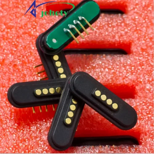
(SMT / SMD) High Speed Pogo Pin. The preferred solution for high-density, low height, automated assembly, and short path high-speed interconnection. Board to board high-speed signal, module to motherboard, low Z-height equipment, batch projects that require automatic mounting.
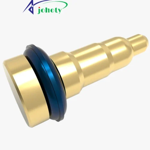
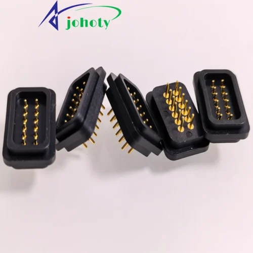
(Through Hole) High Speed Pogo Pin. Suitable for high-speed interconnect solutions that require stronger board end fixation, higher insertion and removal mechanical stability, and more stringent vibrations. Suitable for industrial equipment, vehicle modules, medical equipment, testing fixtures, and frequent plug-in structures.
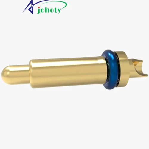
(Right Angle / Horizontal) High Speed Pogo Pin. When vertical entry and exit are not allowed in the space, and when connections must be entered from the side. A high-speed solution for special vertical/parallel docking of two PCBs. Side entry, ultra-thin device, vertical motherboard with daughter board, edge module, and height locked structure.
(Solder Cup) High Speed Pogo Pin. Used for power, charging, quick connect, blind mate systems. Board to wire, module to harness, quick wiring verification, system that requires on-site maintenance and replacement.
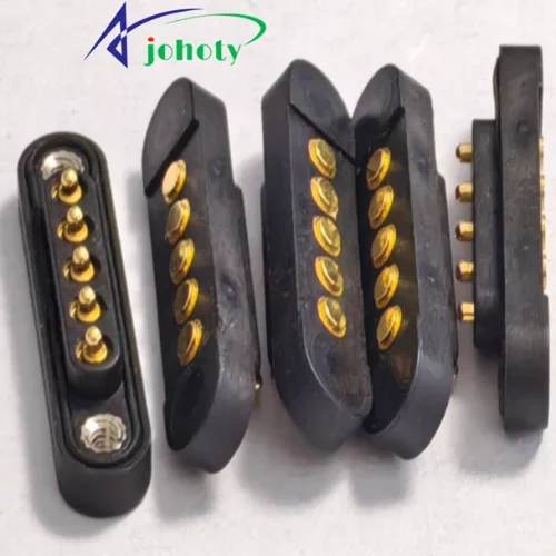
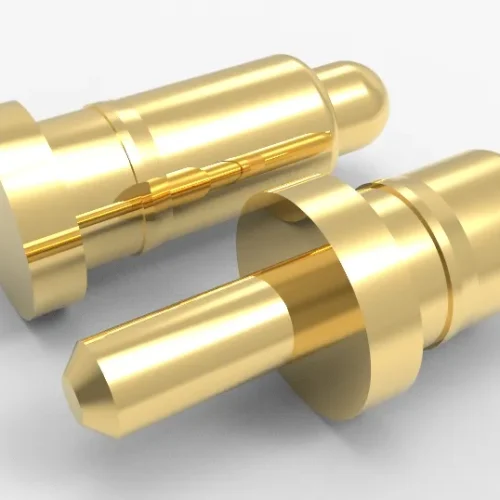
(Double Ended) High Speed Pogo Pin. The core solution for board to board crimping, floating docking, blind insertion, and high-density high-speed splicer. Suitable for high-speed connections between boards, modular stacking, maintainable systems, floating crimping, and high-speed interfaces that require tolerance compensation.
Materials and Manufacturing of High Speed Pogo Pin
Raw materials of high speed pogo pins are not just conductive, but also guided waves. In order to achieve low insertion loss and standing wave ratio (VSWR) at ultra-high frequencies, Johoty abandoned ordinary copper alloys. Adopting a special formula designed specifically for high-frequency signal transmission.
| Part | Materials | Value |
|---|---|---|
| plunger | BeCu | BeCu plunger provides a contact force of >300gf. In 100,000 high-frequency vibration tests, it can tightly adhere to the contact interface. This can effectively avoid signal intermittency caused by micro jitter. |
| barrel | Brass | Brass with high conductivity can mixedly transmit high currents and high-speed signals. With low ground loop impedance,it reduces cross-talk effectively. |
| plating | Gold (Au) and palladium alloy | Middle: Johoty always deposits thick nickel on the copper substrate as a barrier to isolate copper diffusion. |
| Surface: Johoty always deposits A hard gold and palladium nickel alloy coating with a purity of 99.99% and a thickness of 0.1-2.0μm over nickel plating. This can stably control the contact resistance to ≤20mΩ and ensure a complete signal. |
High precision CNC turning and coaxial design:
Craftsmanship: Johoty uses 5 or 6 axis CNC to complete the machining of plunger and barrel in one clamping.
Accuracy: The key dimensional tolerance of the high speed pogo pin is strictly controlled within ± 0.01mm, and can even achieve ± 0.005mm.
High speed value: This precision ensures the continuity of the characteristic impedance of 50Ω. Johoty can ensure minimal changes in the inner diameter of the signal, eliminating signal reflections caused by sudden size changes. Johoty adopts an integrated spiral structure design for high-end high speed pogo pins, integrating springs into the signal path. Significantly reduce the impedance jump caused by multiple contact interfaces in standard pogo pins.
High frequency passivation of springs:
Challenges: Ordinary springs undergo inductance changes during compression, which can affect high-speed signals.
Craftsmanship: Johoty springs are made of SWP-B, SUS631, Inconel, or stainless steel wire. Precision heat treatment and pre-pressing treatment are carried out before assembly to ensure constant spring force. Meanwhile, by optimizing spring helix ratio, it can reduce equivalent series inductance within the operating frequency band. We can ensure the transparency of signal transmission.
Extreme environment verification:
Durability: After 100,000 to 1,000,000 compression cycles, the change in contact resistance is <5%. The signal quality does not deteriorate under long-term use.
Temperature stability: The impedance fluctuations of Johoty high speed pogo pin are effectively suppressed between -55°C and +125°C. Because we accurately matched its material’s coefficient of thermal expansion.
High frequency verification: Johoty can assist customers to work on S-parameters and TDR simulation for each high speed pogo pin. In the frequency band up to 10GHz, insertion loss remains at an extremely low level.
Signal performance and reliability verification of High Speed Pogo Pin
Ultimate signal integrity:
High speed signals are extremely sensitive to impedance mismatch and are the root cause of signal reflection and attenuation. Johoty conducts 3D electromagnetic field modeling and simulation optimization on pogo pins for PCIe and Ethernet.
Accurate impedance matching: Optimize the diameter of the plunger and barrel, as well as the dielectric constant of the insulator material. Implement 50Ω±1Ω characteristic impedance control throughout the entire transmission path to minimize signal reflection.
Ultra-low insertion loss: At 10GHz, the insertion loss can be as low as ≤1.5dB. At 15GHz, insertion loss can still be ≤2.0dB, meeting testing requirements of 5G and autonomous driving radar.
Low crosstalk and interference suppression:
In high-density, fine pitch test sockets, crosstalk between adjacent pins is a hidden killer for high-speed data transmission.
Crosstalk isolation: By optimizing grounding pin layout and structural design, Johoty ensures crosstalk suppression of adjacent channels is ≥40dB at 10GHz. This can reduce the coupling interference between signals to an extremely low level, resulting in high signal purity.
Signal integrity analysis: Combined with eye diagram testing, the eye diagram pass rate is ≥99.9% at 10Gbps. The jitter is controlled within RMS ≤20ps, and the signal remains open during high speed transmission without any errors.
Contact reliability and durability verification:
In addition to electrical performance, the reliability of mechanical connections is the cornerstone of high-frequency testing stability.
Low and stable contact resistance: Johoty uses a hard gold coating of ≥3μm and Pd alloy to achieve an initial contact resistance of ≤20mΩ. After 5,000 to 100,000 connections, the change in contact resistance is ≤10%. This can affect the voltage drop and stability of the customer’s testing signal.
Environmental adaptability: Verified by MIL-STD standard, subjected to 1,000 temperature cycles of -40℃ to +175℃ impact. After 20G vibration test, the contact resistance fluctuation is ≤5mΩ and there is no instantaneous droop. Johoty can ensure absolute reliability of high-frequency signals under temperature changes and vibrations.
Application Highlights of High Speed Pogo Pin
Ultimate signal integrity for lossless transmission:
Ultra-wideband performance: Built for rigorous testing of PCIe and USB4. Johoty high speed pogo pin is not only a conductor, but also an impedance controlled transmission structure.
Extremely low insertion loss: Within critical frequency bands, signal loss is strictly controlled within ≤1.5dB. High frequency signals maintain a purity similar to PCB routing when passing through testing fixtures.
Minimal crosstalk design: Johoty optimizes the layout of grounding pins and internal insulation media. Effectively suppress parasitic capacitance between adjacent high current pogo pins, minimizing the risk of crosstalk. You don’t need to add additional complex shielding layers to meet your testing requirements.
Zero wear contact reduces your total testing costs:
Long cycle life: Johoty adopts a special micro sliding friction design. Generate self-cleaning at the micrometer level upon each contact, piercing through the oxide film. Achieve a stable plugging and unplugging lifespan of over 100,000 times.
Impedance stability: Within a lifespan of 100,000 cycles, the contact resistance remains consistently below 50mΩ. High frequency parameters will not undergo cold welding or sudden changes due to mechanical wear. Significantly reduce the downtime and maintenance time of testing machines.
Ultimate EMC and EMI:
Fully shielded barrel: Unlike low-cost spring loaded pins, Johoty high current pogo pins use a 360° shielded sleeve to tightly wrap the signal pin. This barrel-in-barrel design provides a shielding effect similar to coaxial cables, effectively isolating electromagnetic interference from adjacent channels.
Extremely low EMI radiation: Optimized grounding circuit to minimize high-frequency return path. Significantly reduce EMI noise in the testing environment. It is suitable for consumer electronics RF testing and automotive radar module testing that are extremely sensitive to noise.
Key dimensions for high-frequency optimization:
Customized signal length: Johoty provides a complete set of needle socket solutions from SMT, through-hole reflow soldering to solder cups. The dielectric constant of the commonly used HTN or LCP for each high speed pogo pin connector has been rigorously screened. Ensure precise control of the characteristic impedance from PCB pads to plunger tips within 50 Ω/90 Ω/100 Ω for on-demand customization.
Low dielectric constant: The high speed pogo pin connector uses LCP or PTFE based materials to minimize energy loss of high-frequency signals in the medium.
Performance guarantee for automotive and industrial applications:
Stable operation in a wide temperature range: The working temperature covers from -40°C to +125°C, and can even reach 175°C. It can work in the online testing of the cold/hot shock test chamber as well as vehicle mounted engine compartment. This can maintain stable elasticity coefficient and conductivity performance.
Corrosion resistant coating: Johoty uses ultra-thick gold flash over nickel. Extremely low contact resistance can resist corrosion from high humidity and salt spray. Johoty high speed pogo pin connector meets the reliability requirements for military and aerospace grade testing.
Applications of High Speed Pogo Pin
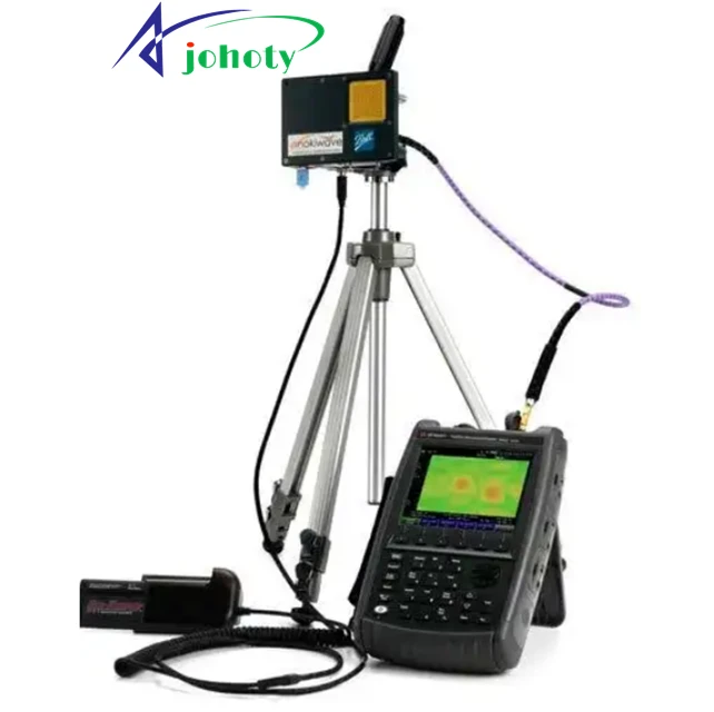
5G millimeter wave base station testing interface:
Challenges: When your chip test stand needs to test 4000 chips per hour at 10GHz, ordinary chips have already begun to resonate. At a high frequency of 10GHz, even small fluctuations in contact impedance can cause signal attenuation >2dB.
High speed pogo pin solutions: Johoty uses high speed pogo pins with palladium plated alloy plunger and beryllium copper springs. It can control impedance fluctuations to <5% at 10GHz, and the eye diagram between ATE devices and chips remains open at all times.
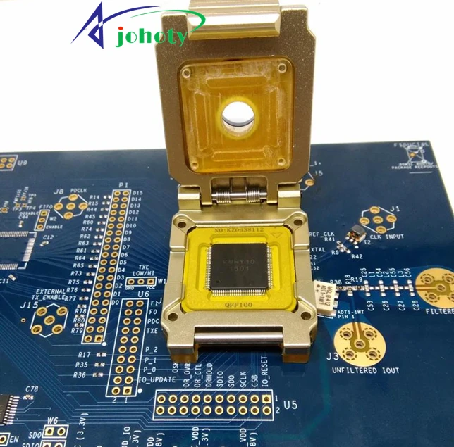
Aging test of OBC chip in autonomous driving vehicle:
Challenges: In vehicle certification, your IGBT or SiC chip needs to work continuously for 100 hours in 125℃aging chamber. Simultaneously carrying 15A current without any contact resistance drift. High temperature, high current, long-term aging, ordinary needles will oxidize and melt plastic.
High speed pogo pin solutions: H-pin or blade pin structures that expand the contact area by 3-5 times through surface contact. Continuously carrying 30A current at 125℃ with temperature rise <20℃ to ensure the validity of aging test data.

High density AR/VR glasses module:
Challenges: On a frame with a length 5.00mm, you need to transmit 5V power, USB 2.0 data, and I²C control signals. The optical module of AR glasses needs to smoothly utilize this data, with the needle tip spacing compressed to 0.15mm. There is signal crosstalk with restraint under this micro spacing.
High speed pogo pin solutions: Johoty uses an array style pogo pin connector with a height difference of 0.20mm between adjacent pogo pins. Add independent grounding pins between signal contacts to suppress crosstalk noise from -30dB to below -45dB.
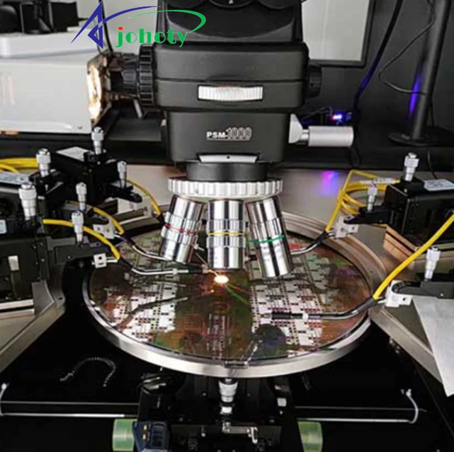
High frequency ATE semiconductor testing:
Challenges: The testing machine needs to be compatible with PCIe 5.0 protocol, with a speed of up to 16GT/s. This requires the connector to be non-reflective. When impedance suddenly changes, a right angle turn will kill the signal.
High speed pogo pin solutions: Johoty uses coaxial layered pogo pins, with the inner layer transmitting differential signals and the outer layer grounded. This forms an accurate 100Ω± 10% characteristic impedance. At the same time, the plunger tip adopts a transition structure of 15° ~ 30° to ensure that the impedance surge is less than 5Ω.

Board to board connections in harsh environments:
Challenges: At the joints of industrial robots, two PCBs need to achieve up to 10Gbps data transmission in a vibrating environment. It needs to withstand extreme temperature differences of -40°C to +125°C and address transient breaks caused by vibration.
High speed pogo pin solutions: Johoty pogo pin with special contact technology features specially designed spring fingers. Can maintain signal path stability even under 20G vibration impact. Supports data rates up to 10GHz and has a 100,000-cycle mechanical lifespan.
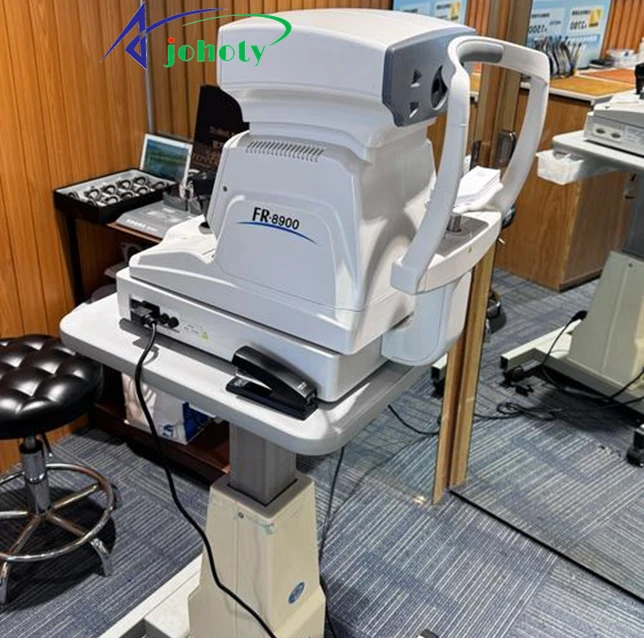
Medical implantable diagnostic devices:
Challenges: Portable ECG monitoring devices require the collection of weak bioelectric signals Any small fluctuation in contact resistance can overwhelm the electrocardiogram signal. The contradiction between biocompatibility and conductivity needs to be resolved.
High speed pogo pin solutions: Johoty uses surgical grade stainless steel or titanium alloy pogo pins with a surface >50μin thick gold coating. The contact resistance remains stable below 50mΩ for a long time and can withstand gamma ray sterilization and disinfection.
High frequency satellite communication module:
Challenges: In low Earth orbit, satellite communication modules need to transmit RF signals in a vacuum environment. Ordinary connectors may be cold soldered or deflated in vacuum, achieving vacuum thermal cycling and ultra-high frequency.
High speed pogo pin solutions: using SMPM compatible pogo pin interfaces. Compensate for changes in dielectric constant in vacuum environment through optimized suspended structures. At 10GHz, the standing wave ratio (VSWR) can achieve ≤1.2.

Immersion liquid cooled servers in data centers:
Challenges: When the server motherboard is immersed in special coolant, you need to establish high-speed PCIe or Ethernet in a liquid environment. Realize the change of liquid dielectric constant characteristic impedance.
High speed pogo pin solutions: Custom pogo pins with fully sealed structures and low dielectric constant ceramic insulators. Maintain 100Ω differential impedance stability under liquid immersion to ensure lossless transmission of signals in the liquid.
FAQ
Geometric structure of impedance matching: Johoty high speed pogo pin isn’t simply cylindrical. The internal plunger, spring, and barrel undergo precise 3D electromagnetic field simulation to form a controlled impedance of 50Ω±3Ω. This can effectively eliminate signal reflections caused by impedance mutations.
Optimization of coatings and materials: Johoty uses high conductivity beryllium copper or palladium copper alloys as substrates and employs selective gold plating or composite electroplating. The contact resistance of <20mΩ will be very easy to achieved. More importantly, at 10GHz, the skin effect of the current is significant. Gold roughness and purity on the surface coating of Johoty high speed pogo pin can greatly reduce high-frequency losses.
Utilization of air medium: Johoty cleverly uses air medium instead of traditional plastic support on key signal transmission paths. Because air dielectric constant is much lower than plastic, this can effectively reduce parasitic capacitance and delay in signal transmission. Thus ensuring the purity and high speed of the signal.
For high-frequency testing, the decrease is unacceptable in electrical performance caused by mechanical wear. Johoty’s solution lies in the collaborative design of mechanical structure and electrical performance:
Unique rolling contact: Traditional pogo pins experience sliding friction during compression, which can easily wear down the coating and generate debris. Johoty adopts a structure of multi-point contact and micro motion rolling. The plugger tip produces slight rolling within a small stroke of contact with the measured point, greatly reducing friction. After 100,000 insertions and removals, you can still see a new contact interface. This design ensures stable contact capacitance and prevents the collapse of the eye diagram due to poor contact.
Non magnetic anti-interference design: The entire high speed pogo pin is made of nickel-free and non-magnetic materials. Thoroughly eliminate interference with high-frequency signal magnetic fields, resulting in extremely high signal purity. In differential signal transmission, it can effectively suppress mode switching.
We fully understand your needs, and what you are describing is the core application of our high speed pogo pin. Our solutions are:
On board chip level packaging compatibility: Johoty provides SMT or through hole high speed pogo pin connectors. Pogo pin design is specifically optimized for high-frequency PCB layout, which can minimize the residual pile effect caused by signal vias.
Low reactance design: Johoty’s unique design of placing spring outside signal transmission can greatly reduce series inductance and parallel capacitance. Our high speed pogo pin bandwidth can easily exceed 10GHz. Fully meet or even exceed the testing requirements of 10Gbps links.
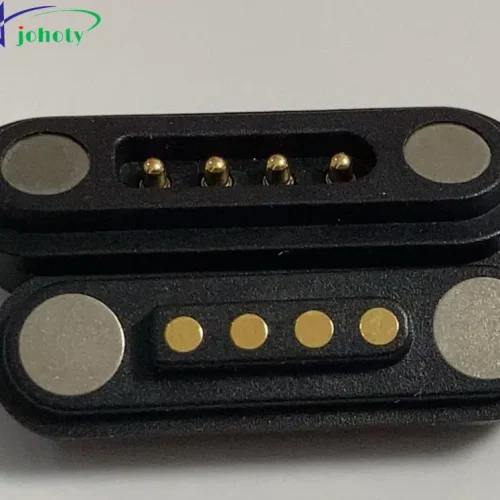
Integration and modularization: Johoty provides customized high speed pogo pin modules. It can directly interface with standard connectors for mechanical and electrical docking. This module can integrate up to 48 high speed pogo pin channels and provide precise alignment. Every blind insertion can be accurately aligned, greatly improving testing efficiency. By choosing Johoty high speed pogo pin, you will have high signal integrity, mechanical durability, and high-frequency testing capabilities. Johoty provides components and customized interconnect solutions. They have been validated through complete 3D electromagnetic simulations and allow you to measure eye diagrams. You will be flawless in every aspect from design to testing.