High Current PCB Connector, 50A Stable Load, 5μm Gold-Plated Pogo Pins, 10mΩ Max. Engineered For Mission-Critical Systems. Contact Us Today!
High Current PCB Connector: A High Current Connection Solution Supporting Critical Systems
High current PCB connectors are commonly used in complex electronic systems with currents exceeding 30A, long continuous power supply times, and high environmental stress. The performance of electrical connection components has shifted from standard parts to the role of system risk controllers. High Current PCB Connector, at the 50A load level, it becomes an indispensable core component in ensuring power integrity.
This article will focus on 50A high current, impedance within 10mΩ, and 5μm gold-plated pogo pin structure as the research objects. Analyze its functional positioning, failure mechanism control, thermal management mechanism, and PCB matching strategy in mission critical systems. And the expected direction of future evolution.
Why is High Current PCB Connector a concern for engineers?
Electric vehicle main control board, industrial grade variable frequency drive, high reliability data center server, drone power relay module. Every high-power system faces a problem: how to maintain sufficient stability in the transmission of high current electrical energy? Should there still be no connection degradation or sudden increase in resistance in response to vibration, temperature rise, contact aging, etc?
The high current PCB connector has become a watershed for the connector industry in terms of high current and high stability.
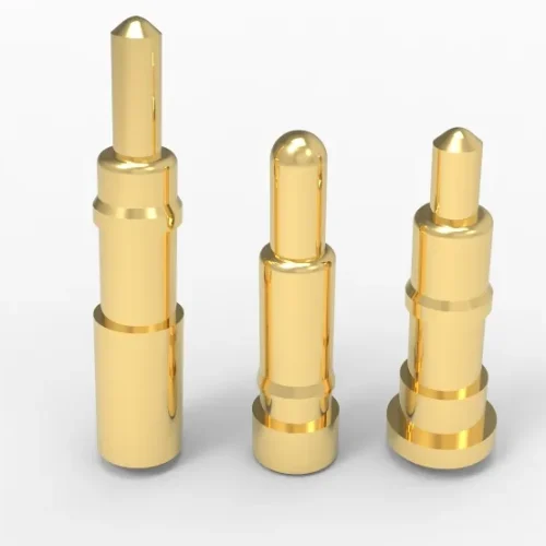
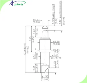
Traditional pin and socket connectors are prone to high temperature hotspots when they exceed 30A due to insufficient contact area, material aging, or elastic fatigue. Even due to the increase in local resistance, carbonization delamination may occur. Johoty’s high-quality gold-plated pogo pin and high current PCB connector with controlled contact resistance within 10mΩ. The optimal solution has been found between mechanical crimping and electrical current flow.
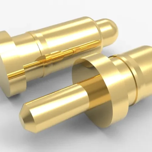
Engineering coupling between Pogo Pin structure and high current carrying
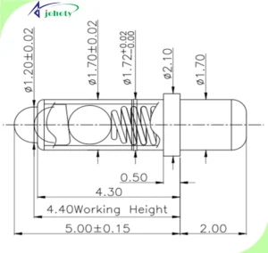
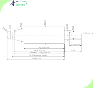
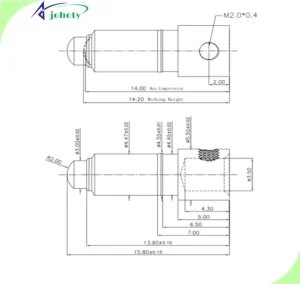
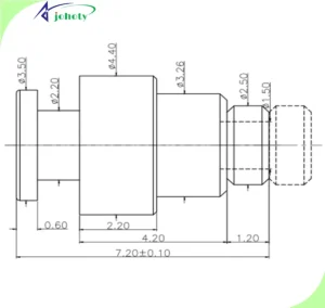
Pogo pins have a different contact structure than traditional plug-in blade or bullet type. It continuously applies axial force to the end point through internal precision springs. Maintain a constant contact pressure under non ideal conditions such as vibration and repeated insertion and extraction.
Johoty is capable of designing and producing current carrying capacities of 50A and above. This directly relates to whether the contact resistance per unit area will increase uncontrollably due to oxide film, micro particles, and micro fatigue. Pogo pin allows for the coexistence of minimum contact surface and maximum elastic recovery in engineering design. Reduce the heat rise at the contact point while ensuring extremely low pressure drop and minimal loss of flow capacity.
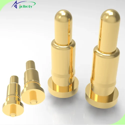
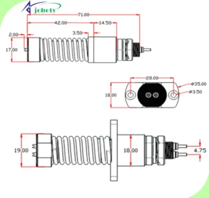
Johoty’s high current PCB connector undergoes the following indicator tests and verifications before leaving our factory:
- Contact resistance should be controlled at ≤ 10mΩ for a long time,
- Fatigue life of the spring is greater than 10,000 compression cycles, or even 200,000 cycles.
- Contact pressure is constant within the range of 1.5N~4.0N (different stroke/stroke control).
Gold plating thickness and long-term reliability: why must it be 5μm?
Gold plating layer with thickness 0.51μm can expose nickel substrate after only 800 hours of arc erosion when passing through 50A current. When gold plating thickness is increased to 5μm, it can smoothly pass high humidity, high temperature, and repeated vibration aging. We also did not observe any obvious exposed points or migration marks.
For electric vehicle power systems, drone flight control modules, and power communication, 5μm gold is prerequisite for long-lasting operation. These devices require high reliability applications that can work continuously for over 1,000 hours. Moreover, high current PCB connectors can effectively slow down:
- Contact point metal migration.
- Corrosion propagation of coating pinholes.
- Localized arc erosion failure.
This is also why many top customers explicitly require a 5μm gold thickness when choosing high current PCB connector.
Structural impact of extremely low impedance (≤10mΩ) on system thermal management
Under a load of 50A, even a contact resistance of 10mΩ means a maximum possible power consumption of 25W (P=I ² R). Lowering this resistor to 5mΩ reduces power consumption by half, opening a safe window for thermal management of the system.
More importantly, the temperature rise behavior at the contact point is exponentially amplified. Its hotspots can induce thermal breakdown of adjacent PCB traces. Thus triggering the unstable state of the entire system nonlinearly. High current PCB connector often requires multiple PIN parallel power supply, multi-layer PCB structure, and limited heat dissipation in narrow spaces. Low impedance is not only an efficiency indicator, but also a system survival indicator.
In the simulation of endpoint temperature rise, the High current PCB connector meets the following requirements:
- 50A@RT The working temperature rise is ≤30℃.
- The area where the thermal diffusion area is greater than or equal to three times the terminal diameter.
- Thermal cycling aging>1000 cycles, with no resistance transition.
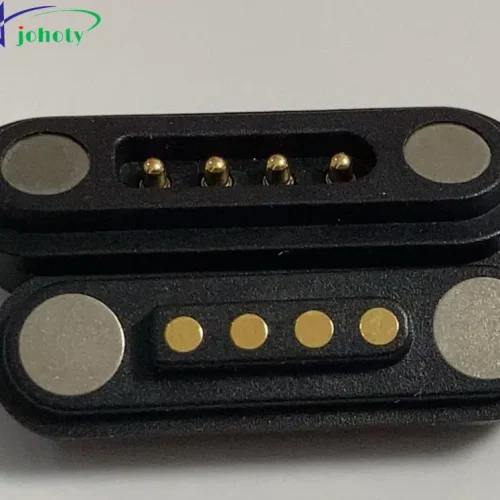
Compatibility with various PCB materials: from FR4 to high-frequency composite boards
In a large number of engineering projects, there is a mismatch in the coefficient of thermal expansion (CTE) between different PCB materials. This affects the long-term stability of the pogo pin connector and the PCB soldering area, as well as the accumulation of micro stresses under thermal cycling.
For this purpose, the high current PCB connector has been optimized in terms of material structure design as follows:
- Support lead-free Sn Ag Cu solder joints without cracking.
- barrel has a buffer structure that is compatible with FR4 (CTE≈16ppm/℃) and PTFE materials.
- The grounding pin supports access to multiple layers of grounding planes to enhance EMI suppression capability.
In complex circuits with high frequency and strong current coexistence, it can operate stably without sacrificing design flexibility through special processes.
Seismic rating and mechanical fatigue life of high current PCB connector
It often faces high vibrations from electric vehicle platforms, lower control cabins of wind power towers, industrial robot arms, etc. The seismic performance of high current PCB connector has become a core concern for many engineers.
The high current PCB connector can pass tests under IEC 60068 and MIL-STD:
- Sinusoidal scanning frequency of 5-500Hz, three-axis resonance without failure.
- Continuous vibration for 10 hours, resistance change ΔR<1mΩ.
- Transient impact 100g@11ms No structural damage.
After soldering on the PCB surface, the barrel axis can still be maintained without deviation, and the elasticity retention rate is greater than 95%. The high current PCB connector provides predictable lifespan model support for mechanical motion platforms.
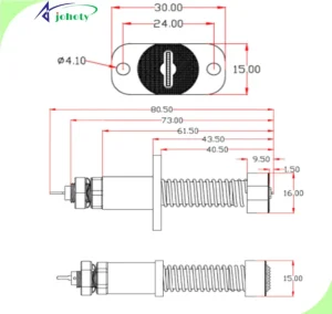
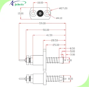
High current PCB connector compatible with standard packaging for contemporary high-speed manufacturing processes
To improve the consistency of SMT and wave soldering production lines in the whole machine factory, high current PCB connectors are commonly packaged using the following process:
- 2D packaging drawings and STEP models are fully compatible with mainstream EDA platforms such as Cadence and Altium.
- Support AOI automatic optical recognition calibration, with a solder pad layout alignment tolerance of ≤0.20mm.
- The packaging method supports multiple feeding mechanisms for Tray/Reel/Tube.
- Recommended PCB thickness: 1.60mm~2.40mm, with a maximum of 12 layers supported.
During the NPI stage of the new model, the high current PCB connector does not require additional process debugging and can achieve rapid mounting and mass production.
Conclusion: The position of High Current PCB Connector in system design far exceeds that of the connection itself
High current PCB connectors are often designed for systems operating under extreme conditions. At this point, each group of high current channels is not an electrical path, but a risk channel. High current PCB connector is no longer an electrical component, but a physical wrapper and barrier for system risks.
Johoty will comprehensively consider structure, materials, coatings, electrical current, thermal control simulation, mechanical tolerances, and process adaptation in engineering. It provides highly controllable connector solutions for system engineers. Make high current channels truly predictable, verifiable, and manageable. If you need a High current PCB connector, Johoty is trustworthy!