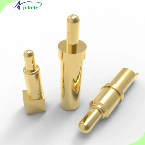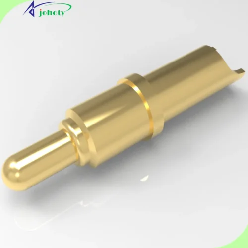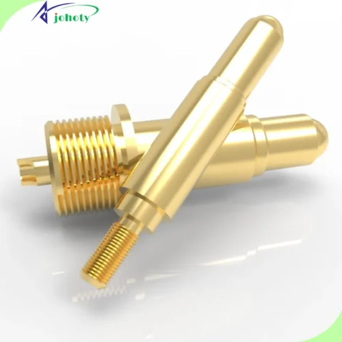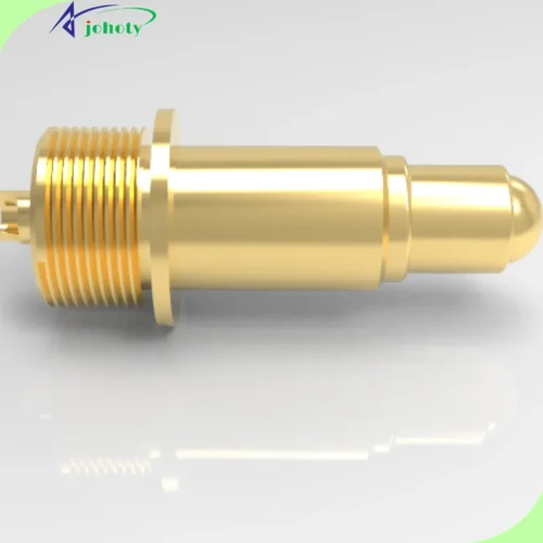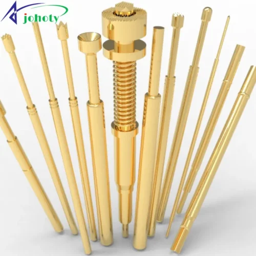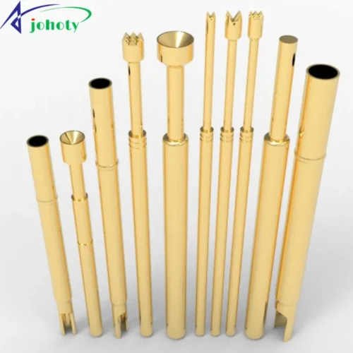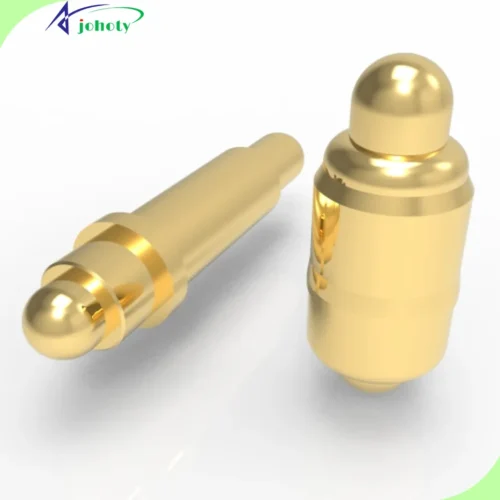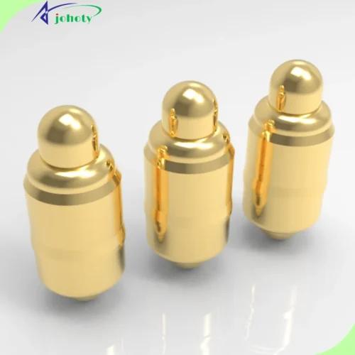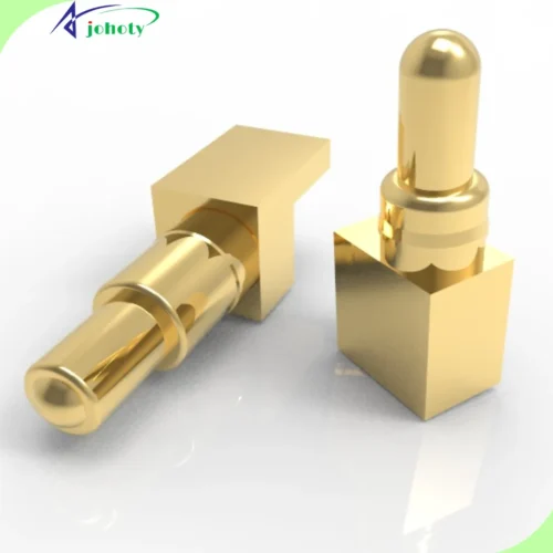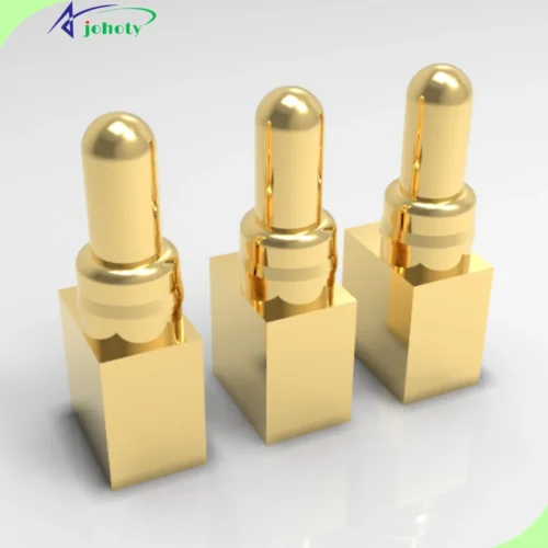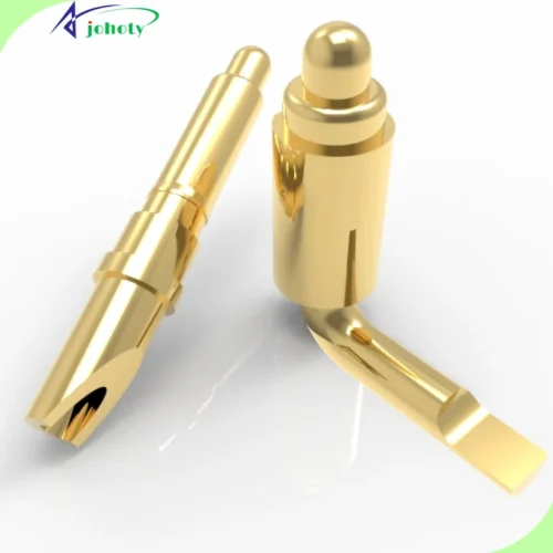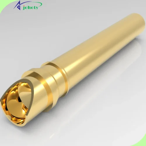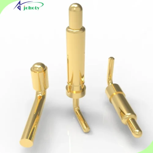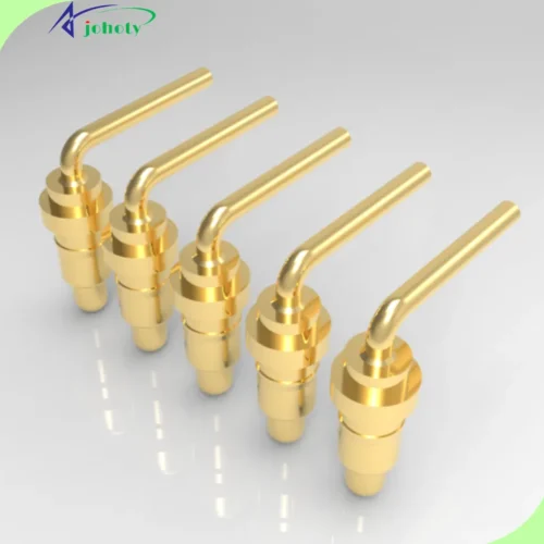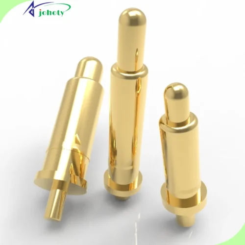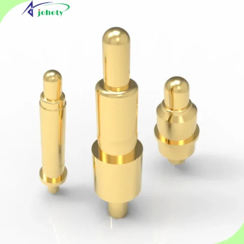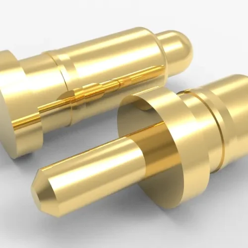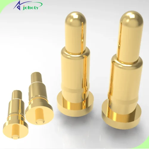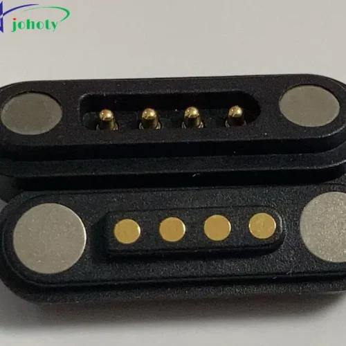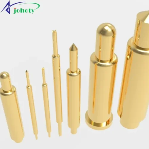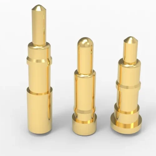
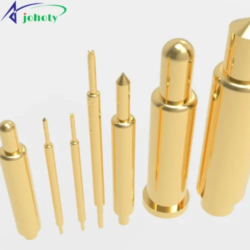
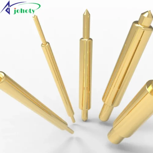
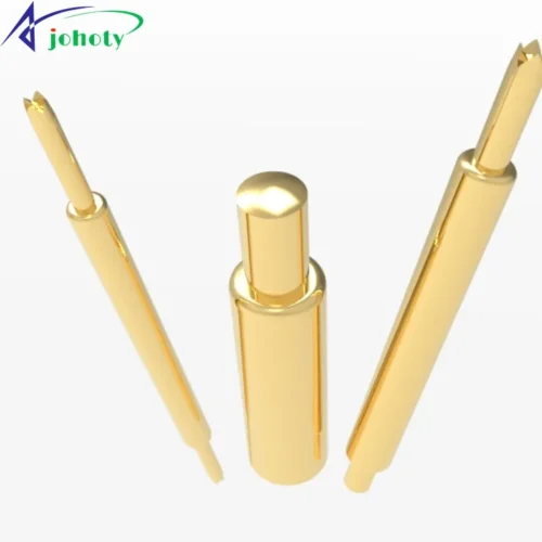
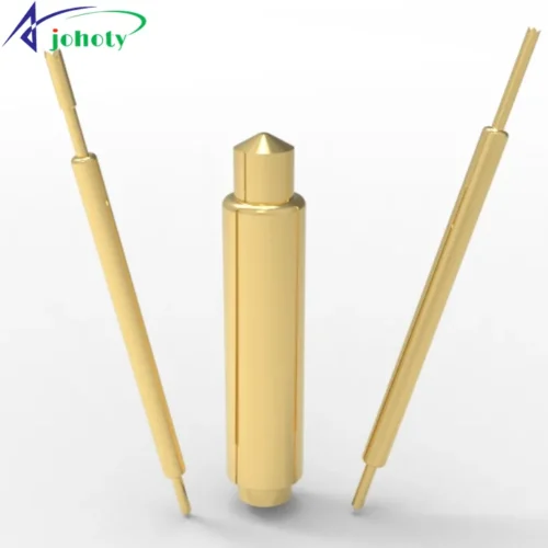
Description of IC chip spring test probes:
Specifications of spring test probes:
Pitch: 0.20mm, 0.35mm, 0.50mm, 0.65mm, 0.80mm, etc
Contact Force: 20–50 gf
Current Rating: 0.5A to 8A @ DC
Resistance: ≤ 50 mΩ, some RF < 10 mΩ
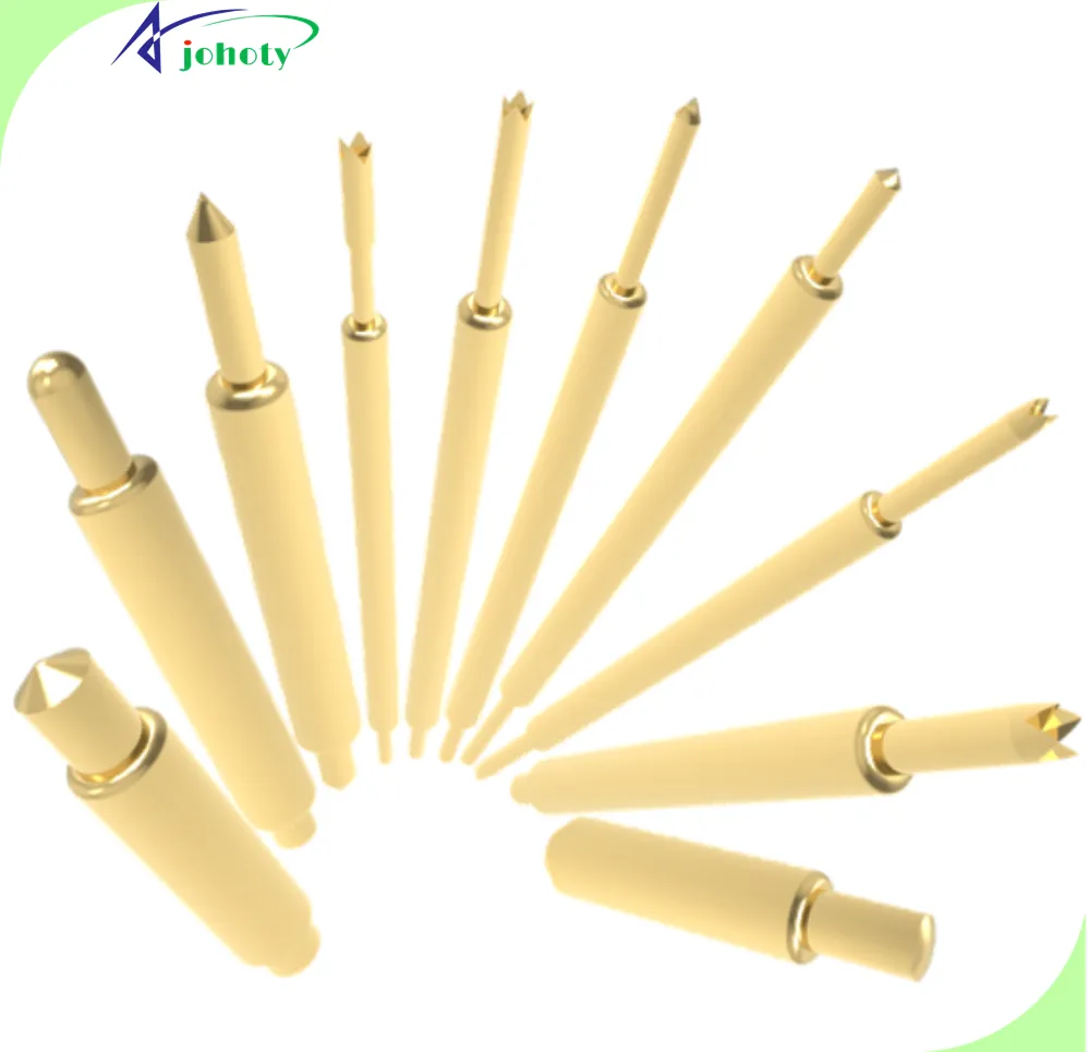
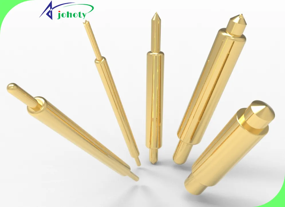
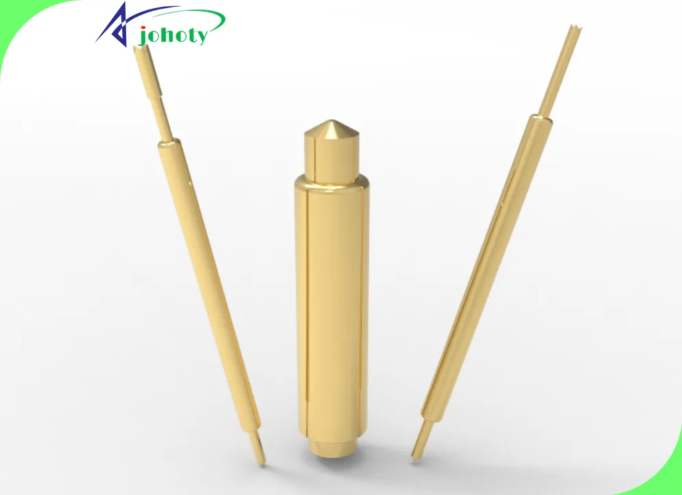
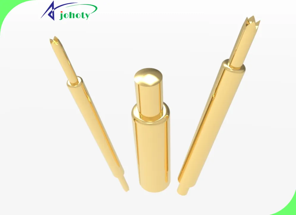
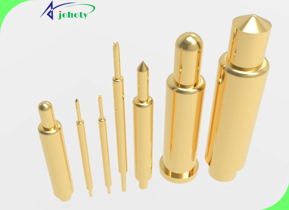
Tip Options: Pointed, flat, coronal, triangular, etc., suitable for solder pads, ball grids, sockets, etc.
Working Stroke: 0.5mm to 2.5mm (providing ultra short stroke to reduce inductance)
Material: Sk4, Beryllium Copper (Au plated)
Operating Temp.: −40 °C ~ +120 °C
Applications of spring test probes:
Use Case: IC final test, wafer test, BGA socket verification
Performance: High-frequency signal integrity > 6 GHz, repeat cycle > 100k times
Compatibility: Suitable for Burn-in boards, semiconductor sockets, pogo pin sockets, IC test fixtures, semiconductor wafer test boards, and precision PCB interface modules.
Catalogs of IC Chip Spring Test Probes:
Challenges and solutions of IC Chip Spring Test Probes:
Test Probes Can‘t Achieve Both Accuracy and Lifetime at the Microscopic Scale
Challenge: When the size of chip pads/bumps reaches the micrometer level, IC Chip Spring Test Probes must maintain precise alignment and stable contact at 10gf+. Traditional test probes are prone to tip wear, deformation, or coating peeling under long-term high-frequency impacts. Causing a surge in resistance and signal distortion, especially fatal in high-speed/RF testing.
Solution: Johoty adopts special alloy and composite coating technology. Composite coating with palladium, cobalt, or rhodium-based alloy as the core material and diamond particle reinforcement. We have achieved the optimal balance between hardness and toughness at the molecular level, extending the lifespan of the probe by 3-5 times. After more than 100,000 tests, it can still maintain micro-ohm-level contact resistance and perfect signal integrity.
Signal Integrity and Interference in High Frequency/High Speed Testing
Challenge: In 5G, millimeter wave, and high-speed applications, IC Chip Spring Test Probes themselves have become part of the transmission line. Inherent inductance and capacitance can severely attenuate high-frequency signals. Causing impedance mismatch, return loss, and crosstalk between adjacent channels. Resulting in significant deviation between test results and actual performance.
Solution: Integrated coaxial shielding and optimized design of dielectric materials. Johoty designed IC Chip Spring Test Probes as miniature coaxial structures. By using the built-in PTFE insulation layer and fully enclosed external grounding shield, the characteristic impedance is stably controlled at 50Ω. This can push the operating frequency above 67GHz and suppress crosstalk below -50dB. Ensure precise high-speed parameter testing directly at the wafer level.
Stability and Consistency Challenges under Complex Operating Conditions
Challenge: Temperature cycling, probe card cleaning agents, and Cu, NiPdAu, SnAg, etc. are often present in the testing environment. This will cause surface oxidation of the probe, accumulation of pollutants, and performance gradient drift. This not only causes fluctuations in test yield, but may also lead to misjudgments of high-value chips.
Solution: Self cleaning plunger tip geometry and environmentally resistant coating. Johoty adopts a scraping or slotted plunger tip design, which can actively scrape off the oxide layer and pollutants every time it comes into contact. At the same time, apply a layer of ultra inert, high-density amorphous carbon on the outermost layer of the coating. Greatly enhance the ability to resist corrosion and adhesion. The fluctuation range (CpK) of contact resistance and pressure is better than 1.67 in 100,000 tests under harsh chemical environments ranging from -55℃ to 150℃.
Why Choose Johoty’s Spring Test Probes?
Johoty’s spring test probes have >10 shapes of plunger tip, flexible custom of length, diameter, strock, force, etc. Worthy of your trust!
Spring Test Probes Benefits:

From the core of performance and accuracy to reliability and authenticity of test data
Johoty solutions: Directly solve this problem by providing spring test probes with low inductance, capacitance, stable impedance, and extraordinary durability.
Huge benefits brought to engineers:
Unparalleled testing accuracy: obtaining real performance data of chips, enhancing research and development verification confidence.
Extraordinary testing stability: significantly reducing false alarm rates and unplanned downtime, directly improving production capacity and yield.

Technical expertise and customization to non-standard and high difficulty testing challenges
Johoty Solution: With a deep collaborative engineering team and agile customized development capabilities, we provide targeted solutions.
Huge benefits brought to engineers:
Accelerate innovation cycle: significantly shorten research and development and validation time, helping customers’ innovative products to be launched faster.

From quality system and reliability + comprehensive cost to constantly rising testing costs
Johoty solution: While providing performance comparable to top brands, optimize total cost of ownership with long lifespan, high consistency, and competitive pricing.
Huge benefits brought to engineers:
Optimized total cost of ownership: achieving lower replacement frequency, less maintenance, and higher equipment efficiency. Show excellent investment returns to management.

From comprehensive cost and supply chain resilience to supply chain fragility
Johoty solution: relying on strong local manufacturing and global layout, providing resilient and flexible supply chain support.
Huge benefits brought to engineers:
Resilient supply chain assurance: the ability to achieve shorter delivery times and respond to unexpected orders. Johoty ensures that the customer’s testing process won’t become a potential production bottleneck.
Spring Test Probes Applications:
Semiconductor Packaging and ATE Automatic Testing
Customer challenge: Transient contact failure occurred in the high-frequency signal port during high cycle testing.
Johoty function: Control the spring stroke of IC chip spring test probes to stabilize within ± 0.02 mm and suppress contact impedance fluctuations.
Customized solution: Adjust the thickness of the spring test probe coating to match different packaging substrates with the geometric angle of the plunger tip.
Problem solving: Avoid virtual connections and signal frame loss to ensure consistency in ATE testing.
Efficiency/Costs: Batch stability rate increased by 22%, and the number of test runs significantly decreased.
Advantages: High frequency characteristics do not degrade, and the lifespan of spring test probes exceeds the industry average by about 2 times.
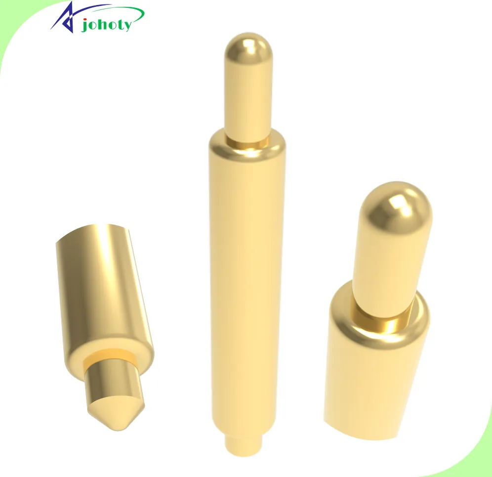
AI accelerates chip yield verification
Customer challenge: Large area BGA packaging is prone to uneven pressure distribution, leading to open circuits.
Johoty function: The elasticity coefficient of the spring test probes accurately matches the thickness of the AI chip carrier board.
Customized solution: Fine tune the stroke and initial pressure of spring test probes to achieve matrix balance.
Problem solved: The fluctuation of the read and write signals converges to the range of ± 3 mV.
Efficiency/Costs: Automated sorting speed increased by 30%.
Advantage: Johoty’s spring test probes support long-term linear stability for ultra-high I/O density testing.

Functional testing of automotive ECU control unit
Customer challenge: Long term high temperature operation leads to fatigue deformation of the test probe.
Johoty function: Use high elasticity fatigue nickel cobalt alloy to maintain the mechanical stability of spring test probes.
Customized solution: Add lateral support slots for spring test probes to prevent displacement.
Solution: Solve the problem of increased contact resistance of spring test probes under temperature drift.
Efficiency/Costs: The average maintenance interval has been extended from March to May.
Advantage: Johoty’s spring test probes have a contact impedance stability of better than ± 2% at high temperatures.

RF and Millimeter Wave Chip Testing
Customer challenge: Signal echo affects S parameter accuracy under high frequency (>20 GHz) conditions.
Johoty function: Maintain impedance matching of Johoty’s spring test probes through coaxial pogo pin structure.
Customized solution: The dielectric constant of the pogo pin core can be customized to adapt to specific frequency bands.
Solution: Reduce S11 echo error by 0.08 dB.
Efficiency/Costs: Reduce testing and calibration time by approximately 35%.
Advantages: The high-frequency signal attenuation is less than 0.3 dB, and the results of Johoty’s spring test probes are more reproducible.
Medical sensor chip measurement
Customer challenge: Microcurrent signals are easily drowned out by environmental noise.
Johoty function: Spring test probes can maintain low contact resistance and reduce parasitic capacitance.
Customized solution: Integrated shielding shell and electrostatic discharge layer.
Problem solved: Control signal drift below 1 µ V.
Efficiency/Costs: Help customers achieve a 15% reduction in test failure rate.
Advantage: Johoty’s spring test probes support stable sampling at the micro current level.
GPU/CPU package heat dissipation verification
Customer challenge: Test probes in the thermal coupling zone experience thermal expansion and displacement.
Johoty function: spring test probes use copper tungsten composite pogo pin cores to control the thermal conduction path.
Customized solution: High thermal conductivity coating improves heat dissipation uniformity.
Solution: Our spring test probes can avoid false triggering caused by temperature differences.
Efficiency/Costs: Increased thermal cycle life by 28%.
Advantage: Johoty’s spring test probes maintain a contact displacement of ≤ 0.01 mm under thermal stress.
DRAM/NAND storage chip sorting machine
Customer challenge: Resistance instability caused by wear of the high-frequency sorting plunger tip.
Johoty function: Control the surface roughness of Johoty’s spring test probes to slow down wear.
Customized solution: The hardness of the ruthenium plating layer is ≥ 850 HV, extending the wear cycle.
Solution: Reduce the error in open circuit determination.
Efficiency/Costs: Annual Spring Test probes replacement frequency reduced by 40%.
Advantage: Johoty’s spring test probes can perform over 500,000 consecutive test cycles.
Signal consistency test of communication interface (SerDes/USB4)
Customer challenge: Mismatched differential line delay affects eye diagram quality.
Johoty function: The mechanical length error of Johoty’s spring test probes is controlled within ± 0.015 mm.
Customized solution: Fine tune the contact force to prevent signal reflection.
Problem solved: The differential signal timing error has decreased to 5 ps.
Efficiency/Costs: Test stability rate increased by 12%.
Advantage: Johoty’s Spring Test probes support high-speed interface consistency of 28 Gbps or more.
Spring Test Probe Advantages:
Customization ability to handle complex scenarios
Advantages: Provides comprehensive solutions from extremely fine spacing (0.2mm) to high current, from high temperature (>150°C) to high frequency, and supports quick customization.
Problem solving: Assist engineers in developing next-generation 3D-ICs, Chiplets, wide bandgap semiconductors GaN, SiC, and miniaturized IoT chips. Johoty can provide previously missing and reliable testing interface solutions to accelerate the launch cycle of innovative products.
Excellent stability and consistency
Advantages: Johoty’s spring test probes (barrels, springs, plungers) are made of SK4 or beryllium copper and undergo special heat treatment. Has extremely high resistance to mechanical fatigue and corrosion. The performance deviation between same batch test probes is extremely small.
Problem solving: Overcoming the core pain points of testing yield fluctuations and misjudgments. Engineers no longer need to calibrate frequently to compensate for probe performance drift. It can significantly improve the efficiency of testing and the accuracy of yield analysis. Ensure that the test data from the first wafer to the 10,000th wafer is highly reliable.
Nano level precision and ultra-long lifespan
Advantages: Adopting ultra precision grinding plunger tips to achieve non-destructive contact. SUS631 spring mechanics design and selected materials ensure extremely low performance degradation after 500,000 testing cycles.
Problem solving: Johoty’s spring test probes have completely solved the problems of scratches, contamination, and decreased test consistency caused by test probe wear. Significantly reduced the repair rate and maintenance downtime of the test bench. Provide a stable foundation for long-term high-throughput mass production testing (high-volume manufacturing) and rigorous reliability verification.
Ultimate electrical performance
Advantages: Ultra low and stable contact resistance (<20m Ω), excellent current carrying capacity (up to 7A+), and a bandwidth of up to 50GHz.
Problem solving: IC chip spring test probes fundamentally eliminate signal integrity issues, resistance thermal noise, and current bottlenecks during the testing process. Engineers can fully trust the accuracy of test data. Obtain true performance during high-speed SerDes, RF, and high-voltage high current power device testing.
FAQ
Johoty solution: Customize the electromagnetic performance of IC chip spring test probes.
Extremely low inductance (<1nH) and shielding options: minimize signal attenuation and delay.
Exclusive dielectric material coating: effectively isolates and reduces crosstalk between adjacent spring test probes.
Accurate impedance matching (such as 50 Ω): ensures the transmission of high-frequency signals without reflection, ensuring testing accuracy.
Johoty solution: Customize the mechanical and material properties of IC chip spring test probes.
Ultra long working life (100,000~500,000 cycles): using high-strength and wear-resistant tungsten rhenium alloy plunger tips and SUS631 precision springs.
Extremely low contact resistance and resistance fluctuations: ensuring long-term consistency and reliability of test readings.
Excellent anti jamming structure design: suitable for high-speed automated testing or high-precision testing instruments, minimizing downtime maintenance.
Johoty solution: Customize the geometry and strength of spring test probes.
Rich customization of plunger tip shapes: from pointed cones to pyramids, flat shapes, 3 claws, 4 claws, 9 claws, accurately matching different pads/solder balls.
Precise elasticity control range (such as 5gf to 200gf+): Spring test probes ensure reliable contact while avoiding excessive pressure damage to brittle solder balls or circuits.
Small spring test probe diameter and high-density arrangement capability: easily cope with micro spacing (as low as 0.20mm) challenges, achieving comprehensive coverage testing.