High Vibration 9X Pogo Pins Deliver Secure PCB Connections, 10mΩ Resistance, 5μm Gold Plating, Zero Contact Failures In Motion. Know It Now!
Introduction: Challenges of Electronic Connections under High Vibration
High vibration often occurs in electronic systems under high-frequency motion, impact, and vibration conditions. Therefore, connectors in high vibration often become the most vulnerable part in engineer design. Traditional connection designs rely on solder joints, patches, or elastic structures to maintain the continuity of electrical signals. But in connections with obvious mechanical interference, engineers often find intermittent contacts. Ultimately causing system logic errors, transient power outages, and even functional downtime of the customer’s equipment.
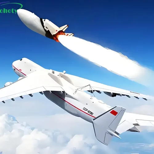
The unmanned aerial vehicle of the American guest experienced sustained high g-value acceleration and resonant oscillations during flight. It is highly likely to cause micrometer level contact displacement within the connector. Similar challenges repeatedly appear in different forms in radar modules, medical imaging equipment, and rail transit signal systems.
Therefore, customers often request Johoty to design pogo pins with high redundancy, low impedance, strong structural constraint, and shock resistance. This pogo pin connector, which can be used for high vibration, has become a common demand among high-end electronic system manufacturers.
Essence and Cause Analysis of High Vibration Contact Failure
Contact failure does not necessarily manifest as physical fracture, it is often an invisible failure mode. Mainly due to the following reasons:
Fretting corrosion: Repeated vibrations cause metal migration on the surface of the plunger tip, increasing contact resistance.
.
Contact bounce: The plunger tip cannot provide sufficient pre pressure stably.
Particle pollution and oxidation: In thin coating designs, high vibration can easily lead to unstable pogo pin signals due to oxidation.
Thermal stress-induced deformation or stress relaxation: Structural degradation caused by material creep under alternating high and low temperatures.
Johoty’s pogo pin connector fundamentally solves the above problems. The structure of multi-point parallel connection and customized travel constraints improves the overall stability and redundancy margin against failure.
High Vibration Core Indicator: How to achieve 10mΩ contact resistance?
It is not easy to achieve a stable resistance value of ≤ 10mΩ in pogo pin. The key parameters include:
Spring design: It needs to have low deformation rate and high rebound rate (using SWP-B, BeCu, SUS), and undergo life curve screening.
Contact surface morphology: The top shape needs to be optimized as a convex point or spherical cap to reduce the pressure per unit area.
Uniformity of electroplating: The 5μm gold coating is chemically plated and polished to ensure that micro and nano particles do not excessively accumulate, leading to an increase in local resistance.
Welding area distribution: The PCB welding area inside the module should avoid micro cracks or cold welding to form a truly low resistance path.
In addition, multi round step load verification was conducted in IEC and MIL-STD. After running 100,000 cycles at 1A current, the contact resistance of the pogo pin connector does not change by more than 2mΩ.
Correlation between gold plating thickness and durability: process basis for 5μm parameter
Most spring loaded pins or conductive spring blades on the market only use a gold layer thickness of 1 μin-3 μin. Cost and processing convenience are the main driving factors. However, in high-frequency connections, the wear resistance and corrosion resistance of the gold layer directly determine the operating life of your equipment system.
The advantages of a 5μm gold layer mainly include:
Reduce the probability of micro motion wear: Even in a micro slip state, there is still enough sacrificial layer to be consumed with a thickness of 5μm.
Prevent substrate exposure: prevent Ni or Cu layer from oxidizing and diffusing to the contact surface.
Improving conductivity: The thicker the gold layer, the more pure gold interface is formed on the contact surface, and the electron mobility is increased.
Compatible with multiple reflow soldering or wave soldering environments: The gold layer will not delaminate or coarsen due to high temperature.
The 5μm gold layer is not derived from commercial compromise, but from optimization results based on environmental lifetime analysis (HALT+HASS). It can demonstrate ultra-high conductivity and contact durability in connections under high vibration.
High vibration simulation testing and verification
Pogo pin connector was designed with reference to the following real-world applications for high-frequency impact testing:
UAV flight control board: frequency is 70-300Hz, acceleration is 3-6g, continuous operation for 48 hours. Result: No contact loss, contact resistance change ≤1.5mΩ.
Industrial LiDAR scanner: horizontal resonance + vertical drop combined testing. One failure in multiple pogo pins does not affect the overall stability of signal transmission.
Vehicle mounted rail transit communication module: temperature -40~+85℃, humidity alternating 95% RH@60℃, 500h. No oxide deposition, no short circuit or open circuit occurrence.
These tests were conducted by the client’s laboratory in accordance with ISO 16750 and IEC 60068 standards. Verified the robustness of pogo pin connector under complex mechanical disturbances.
Reliability of PCB design integration angle
Pogo pin connectors often require PCB layout, pad design, and structural fixation to improve overall connection reliability. It is a variable that must be considered during integration in the early stages of system design.
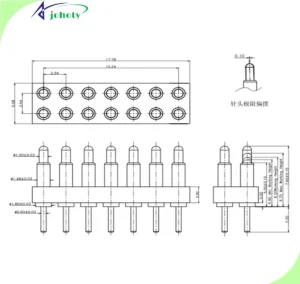
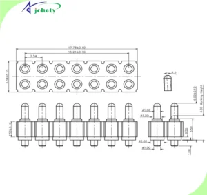
The following are typical integration parameter suggestions for pogo pin connectors:
Pad size: It is recommended to have a diameter of ≥1.2mm to ensure the welding contact area and thermal conductivity efficiency.
Solder plating: ENIG or thick gold treatment can reduce the risk of micro corrosion.
Coordination force simulation: Through FEM simulation, the stress concentration on the PCB does not exceed 60MPa, avoiding the generation of micro-cracks.
Module fixation: Double positioning with screw limit and structural adhesive can be used to eliminate relative motion during high vibration.
Via and wiring: Blind hole structures should be avoided in signal areas to reduce high-frequency losses and stray inductance effects.
The above design can be simulated and confirmed on a high vibration table through actual samples. Further optimize the durability and connection durability distribution of Pad using statistical methods.
PCB structural response and connection stress under high vibration
In high vibration, structural coupling resonance is one of the core risks leading to connector failure. The contact surface between the connector plunger tips and the PCB bears alternating loads of shear force and positive pressure during vibration. The following phenomena are prone to occur:
The solder pad is raised or peeled off (especially on multi-layer boards). Lateral sliding of the pins causes non aligned contact. The contact area is subjected to micro fatigue damage, resulting in the formation of micro-cracks.
Based on FEM simulation and experimental data, the characteristics of pogo pin connector in 3-10g and frequency range of 20-300Hz are as follows:
The equivalent stress distribution is more uniform: each pogo pin bears a smaller unit force, greatly reducing single point fatigue.
Elastic pre stress absorption: The spring loaded pin’s internal spring achieves dynamic stroke adjustment to avoid concentrated force accumulation.
Structural synchronized rebound: prevent contact misalignment caused by asynchronous displacement rhythms of different pogo pins.
From the perspective of PCB design, pogo pin connector effectively reduces the accumulation of peak stress at a certain point. Greatly improves the reliability of PCB connection areas under high vibration.
Signal distortion caused by high vibration and compensation path of Pogo Pins
Pogo pin connectors not only face mechanical challenges under high vibration, but also bring electrical interference:
- Micro motion contact resistance fluctuation, current density disturbance.
- Micro gap variation at contact points, parasitic inductance variation.
- Transient bounce effect, loss/delay of digital signal pulses.
Johoty’s pogo pin connector has two key strategies to address these issues:
Physical contact redundancy: Multiple contact points can effectively disperse the current path. Some points experience transient disconnection due to vibration, while the remaining contact points can still provide signal pathways. Reduce the probability of signal loss.
Electrical performance stabilization strategy: Independent preload setting for each Pogo Pin+seismic structural compensation stroke (± 0.2mm). The total equivalent contact resistance fluctuation is within ±0.5mΩ. The impedance curve variation amplitude within the frequency range of 1MHz~50MHz is less than 5%, ensuring the consistency of high-speed signals.
Pogo pins can still meet the requirements of industrial Ethernet under high vibration RS-485, Connection requirements for high-frequency ADC interface.
Material response and Pogo pin structural stability under high vibration
Unlike static fatigue testing, vibration and impact pose extremely high challenges to the material composition and structure of pogo pin connectors. Under the action of multi axis vibration, falling, explosion, and sudden braking:
- Conventional spring loaded pins may experience bottom out travel due to instantaneous acceleration, resulting in elastic failure at the contact point.
- Micro peeling phenomenon occurs at the interface between the coating and the spring separation.
- The insufficient yield limit of the housing material causes the Pin array to deflect, resulting in nonlinear deflection.
To solve such problems, we adopt the following approach when designing pogo pin connectors:
- Precise limit mechanism to prevent internal shaping caused by overtravel.
- Heterogeneous material layered structure: BeCu is for the spring part to enhance fatigue resistance, and high-purity copper is for the plunger tip to improve conductivity.
- The housing adopts modified PPS or LCP composite materials, which improve impact resistance by more than 40%.
- Pre embedded reinforcement ribs are used in the injection molded parts of the module to prevent the parallelism of the pogo pin array from losing control after vibration.
During 50 free drops of 1.5m and 3-axis impact tests at 6g/150Hz, the pogo pin connector maintained its intact structure and the signal remained stable.
Conclusion: The Engineering Frontier of High Vibration Application Connectors
The greatest significance of Pogo pin connector is that it provides a highly reliable physical connection solution for electronic systems in the event of dynamic loss of control. Its technical feature lies not in having a few more pogo pins than others, but in:
- Multi point dynamic compensation design under high vibration.
- Structure material electrical performance synergistically resist high vibration.
- The verification path is under real high vibration conditions, rather than ideal laboratory scenarios.
The reliability requirements for pogo pin connectors are constantly increasing in unmanned systems, rail transit industry, aerospace, and high mobility platforms. Traditional design methods are no longer sustainable. And Johoty’s anti high vibration pogo pins are the reliable standard for your effective connection.